Saturn PCB Toolkit (V8.02) PCB Design Calculator for Trace Width, Via Current and Impedance Download
Summary
Saturn PCB Toolkit is a freeware desktop application for PCB-related calculations that PCB designers and engineers regularly need. Unlike online calculators that require internet access and may use outdated formulas, this toolkit provides a comprehensive suite of engineering tools including trace width vs current capacity (per IPC-2152), via current analysis, differential pair impedance, padstack calculations, crosstalk estimation, and much more. The software does not use Java and is not subject to the Log4j vulnerability.
The toolkit is developed by Saturn PCB Design, Inc. and has been continuously updated based on customer feedback. Version 8.02 includes over 30 different calculators covering microstrip and stripline impedance, differential pairs, via properties, conductor current capacity, planar inductors, padstack dimensions, crosstalk, Ohm’s Law, reactance (XC/XL), BGA land patterns, effective dielectric constant (Er Eff), wavelength, PPM for crystals, fusing current, thermal management, power delivery network (PDN) impedance, and embedded resistors.
Key Features
1. PCB Trace Width and Current Calculator
Calculates the current a conductor needs to raise its temperature over ambient per IPC-2152. Now also calculates DC resistance with temperature compensation. Other conductor properties include skin depth, voltage drop, DC resistance, power dissipation, and bandwidth.
2. PCB Via Current Calculator
Calculates the current a via needs to raise its temperature over ambient per IPC-2152. Other via properties include capacitance, inductance, impedance, step response, DC resistance, resonant frequency, thermal resistance, voltage drop, and power dissipation in dBm.
3. Differential Pair Impedance Calculator
Calculates differential pair impedance for balanced lines. Supports edge coupled differential pair, edge coupled internal symmetric/asymmetric, edge coupled embedded, broadside coupled shielded and non-shielded differential pairs.
4. PCB Conductor Impedance Calculator
Calculates impedance of microstrip, embedded microstrip, stripline (symmetrical, asymmetrical, dual), and coplanar waveguide structures. Includes frequency-dependent Er effective calculation.
5. Via Properties Calculator
Comprehensive via analysis including via current (IPC-2152), capacitance, inductance, impedance, DC resistance, resonant frequency, step response, thermal resistance, and differential via analysis. Includes microvia support and aspect ratio limit checking.
6. Padstack Calculator
Calculates outer and inner layer pad diameters given drill size. Includes BGA land calculator per IPC-7351A specification, conductor-to-pad clearance, conductor-to-BGA land breakout, corner-to-corner distance, and 2-conductor routing analysis.
7. Planar Inductor Calculator
Calculates inductance for square, hexagonal, octagonal, and circular planar PCB inductors using the modified Wheeler formula. Uses turns, conductor width, spacing, and outer radius.
8. Crosstalk Calculator
Calculates coupled voltage between two conductors based on rise time, voltage, length, and spacing. Also includes NEXT (Near-End Crosstalk) calculation in the differential pairs tool.
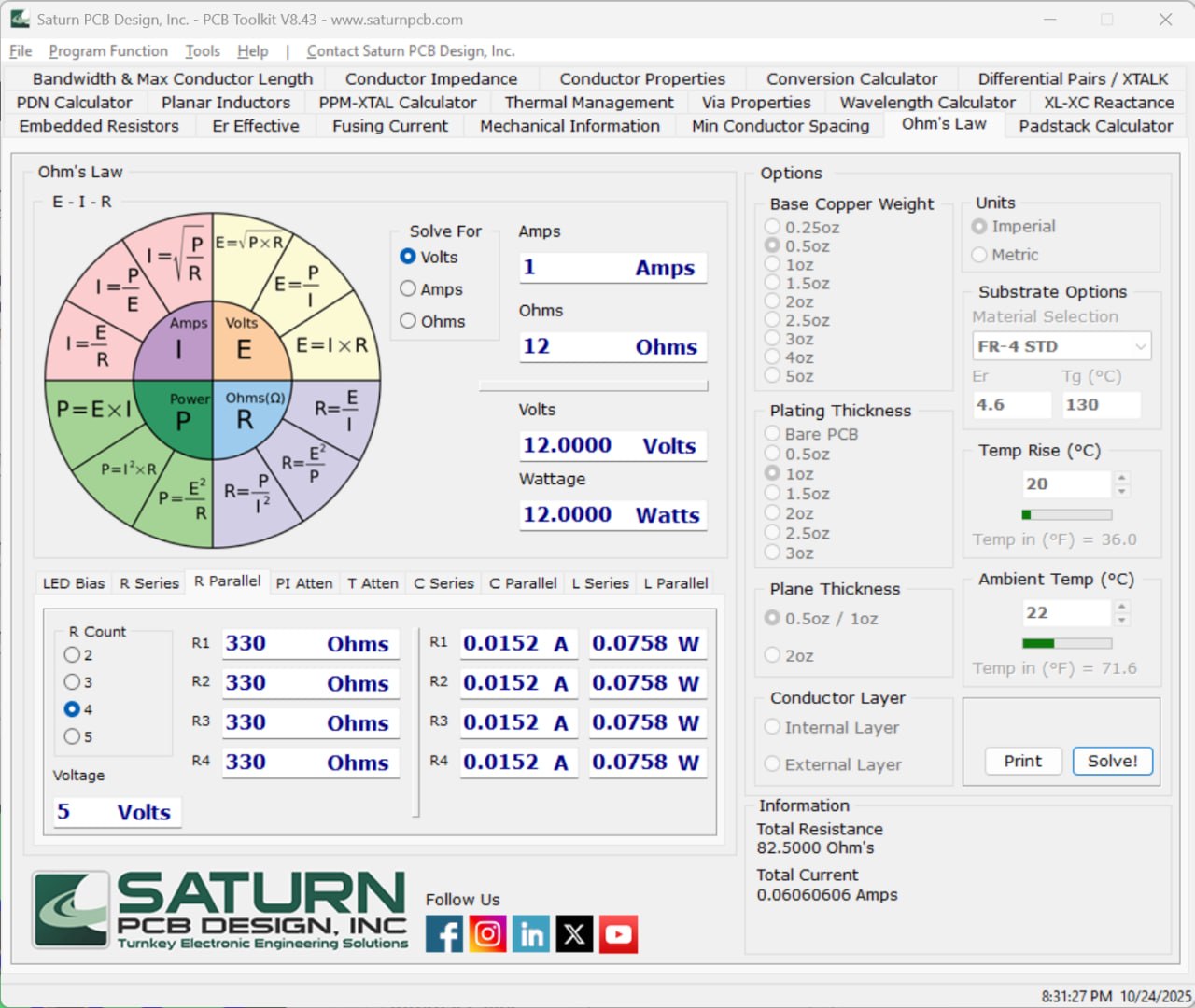
9. Ohm’s Law and Reactance Calculators
Ohm’s Law calculator with LED resistor sizing, resistor divider, PI pad, T pad, and series/parallel RLC configurations. XC/XL reactance calculator with resonant frequency determination.
10. Minimum Conductor Spacing Chart
Calculates minimum conductor spacing using peak AC or DC voltage based on IPC-2221C data. Includes device type selection (bare board or assembly).
11. Fusing Current Calculator
Uses Onderdonk’s equation to determine the fuse current of a conductor based on width and time duration. Includes multiplier adjustment for improved accuracy.
12. Thermal Management Calculator
Calculates device junction temperature using thermal resistance and power dissipation. Also calculates heat sink junction temperature.
13. Power Delivery Network (PDN) Impedance Calculator
Calculates target PDN impedance based on voltage rail, maximum current, transient percentage, and maximum AC ripple. Also includes plane capacitance calculator.
14. Effective Dielectric Constant Calculator
Uses the E. Hammerstad and O. Jensen equation to determine effective dielectric constant of a microstrip.
15. Wavelength and Bandwidth Calculators
Calculates wavelength using Er Eff and frequency/period. Calculates maximum trace length before transmission line effects using IPC-2251 method or frequency domain method.
16. Conversion Tools
Units conversion (mm to mils, mils to mm), temperature conversion (C to F, F to C), dB to voltage gain, rectangular to polar conversion, and angular conversion (degrees to radians).
17. PPM and XTAL Calculator
Calculates XTAL capacitor values based on load and stray capacitance. Converts between PPM and Hertz for crystal oscillator frequency variation.
18. Mechanical Data
Wire gauge chart (AWG) with diameter, resistance, and max amps. Drill chart with imperial and metric diameters. Screw thread size chart (imperial and metric).
What’s New in Saturn PCB Toolkit V8.02
- Version 8.02 includes multiple enhancements over previous versions.
- Added changed current density output units and updated software signing cert.
- Updated Minimum Conductor Spacing to IPC-2221C.
- Added Import/Export function and increased number in RLC series/parallel calculator to 5.
- Added microns option, Crosstalk Calculator (unsupported), and wire voltage drop.
- Changed default install directory to Program Files (x86) and added permissions to help with registry issues.
- The V8 series no longer uses multipliers for cross sectional area as related to IPC-2152, improving accuracy.
System Requirements
To run Saturn PCB Toolkit V8.02 effectively, your system should meet the following specifications.
Minimum Requirements:
-
Operating System: Windows 7, Windows 8, Windows 10, or Windows 11 (32-bit or 64-bit)
-
Processor: Any Intel or AMD processor
-
RAM: 1 GB minimum (2 GB recommended)
-
Storage: 50 MB free space
-
Display: 1024 x 768 resolution
-
Additional: .NET Framework (installed automatically if needed)
Installation Guide
Follow these steps to install Saturn PCB Toolkit V8.02.
-
Download the Installer: Obtain the official Saturn PCB Toolkit installer from the Saturn PCB Design website.
-
Try Before You Buy: The software is completely freeware, with no trial limitations, no cost.
-
Verify System Compatibility: Ensure your Windows version is supported.
-
Close Other Applications: Close any other engineering or calculator software.
-
Run as Administrator: Right-click the installer and select “Run as Administrator.”
-
Follow the Setup Wizard: Complete license acceptance and installation directory selection (default is Program Files (x86)).
-
Launch Saturn PCB Toolkit: Open the software from the desktop shortcut or start menu.
-
Select Units: Choose Imperial (mils) or Metric (mm) from the General Settings.
-
Configure Material: Select PCB substrate (FR-4, RO4003, etc.) or enter custom dielectric constant and Tg.
-
Start Calculating: Use tabs for different calculators Conductor Properties, Via Properties, Differential Pairs, etc.
How to Use Saturn PCB Toolkit
Step 1: Set General Preferences
Click the Options button. Select Imperial (mils) or Metric (mm) units. Choose base copper weight and plating thickness. Select PCB substrate material (FR-4, etc.). Set ambient temperature and desired temperature rise.
Step 2: Calculate Trace Width for Current
Go to Conductor Properties tab. Ensure IPC-2152 without modifiers is selected (default and recommended). Enter conductor width (or solve for width by checking “Solve for Conductor Width”). Select conductor layer (external or internal). Set plane presence and distance. Enter current requirement. The tool calculates required trace width, temperature rise, DC resistance, voltage drop, and power dissipation.
Step 3: Calculate Via Current Capacity
Go to Via Properties tab. Select layer set (2-layer, multi-layer, or microvia). Enter via hole diameter (finished diameter). Set internal pad diameter and reference plane opening (for multi-layer). Enter via height (PCB thickness). Set plating thickness. Enter temperature rise. The tool calculates via current capacity, capacitance, inductance, impedance, DC resistance, and thermal resistance.
Step 4: Design Differential Pair
Go to Differential Pairs tab. Select coupled pair type (edge coupled, broadside coupled, etc.). Enter conductor width (W), spacing (S), and height (H). Set target differential impedance (e.g., 100 ohms for USB, 90 ohms for Ethernet). The tool calculates Zo, Zdiff, Zeven, Zodd, and indicates when within tolerance.
Step 5: Calculate Padstack Dimensions
Go to Padstack Calculator tab. Select hole type (thru-hole or BGA). For thru-hole: enter hole diameter, minimum annular ring, pad style (plated/non-plated). The tool calculates external layer pad diameter, internal signal layer pad diameter, internal plane layer pad diameter, and thermal spoke width. For BGA: select nominal ball diameter, the tool calculates nominal land diameter and land variation per IPC-7351A.
Step 6: Calculate Minimum Conductor Spacing
Go to Minimum Conductor Spacing tab. Select voltage between conductors (0-15V, 16-30V, 31-50V, 51-100V, 101-150V, 151-300V, or custom). Select device type (bare board or assembly). The tool displays minimum spacing per IPC-2221C.
Step 7: Additional Calculations
Use other tabs as needed: Ohm’s Law for LED resistors and attenuators, Reactance for XC/XL, Planar Inductors for PCB coils, Crosstalk for coupled voltage, PDN Impedance for power delivery analysis, Thermal Management for junction temperature, and Fusing Current for overload protection.
Best Use Cases
| Use Case | Calculator | Key Benefit |
|---|---|---|
| High-current PCB Design | Trace Width + Via Current | IPC-2152 compliant traces and vias |
| High-speed Digital | Differential Pairs + Impedance | 90/100 ohm matching, crosstalk control |
| RF/Microwave Design | Microstrip/Stripline + Er Eff | Accurate impedance control |
| BGA Breakout Routing | Padstack + BGA Land Calculator | Max trace width between lands |
| Power Electronics | PDN Impedance + Plane Capacitance | Target impedance, decoupling requirements |
| LED PCB Design | Ohm’s Law (LED bias) + Thermal | Resistor sizing, junction temperature |
| PCB Fabrication Documentation | Padstack + Drill Chart | Gerber-ready pad dimensions |
Advantages and Limitations
Advantages:
- Saturn PCB Toolkit is completely freeware with no trial limitations or cost.
- It supports the latest IPC standards (IPC-2152 for conductor current, IPC-2221C for spacing).
- The V8 series no longer uses multipliers for cross-sectional area, improving accuracy.
- The toolkit includes over 30 calculators in one application.
- All calculations are offline, no internet required. The software does not use Java and is not subject to Log4j vulnerability.
- Comprehensive via analysis includes capacitance, inductance, impedance, step response, resonant frequency, thermal resistance, and current capacity.
- Differential pair calculators support edge coupled, broadside coupled, and multiple differential structures.
- Padstack calculator supports thru-hole, BGA, and multi-layer pad dimensions with thermal relief suggestions.
- Conductor spacing per IPC-2221C includes device type selection. Regular updates based on user feedback ensure continued improvement.
Limitations:
- Saturn PCB Toolkit is Windows-only with no native macOS or Linux version.
- Some advanced features (differential via calculator, anisotropic calculations) may require deeper engineering knowledge.
- The software encourages use of IPC-2152 without modifiers for most applications, but modifiers may be needed for trace width minimization.
- Crosstalk calculator is noted as unsupported by the developer.
Alternatives to Saturn PCB Toolkit
| Software | Best For | Key Difference from Saturn |
|---|---|---|
| EEWeb PCB Calculators | Web-based quick calculations | Free but requires internet, less comprehensive |
| UltraCAD PCB Calculators | Trace width and impedance | Free but limited calculators |
| KiCad PCB Calculator | Open-source PCB design integration | Free, integrated with KiCad, fewer calculators |
| Polar Instruments Si8000 | Professional impedance | High cost, more accurate, industry standard |
| Keysight ADS LineCalc | RF/microwave | Professional, expensive, broader RF focus |
| Manual math + spreadsheets | Custom calculations | Free but time-consuming, error-prone |
Frequently Asked Questions
Q1. Is Saturn PCB Toolkit really free?
Yes. Saturn PCB Toolkit is completely freeware with no trial limitations, no ads, and no cost.
Q2. What IPC standards does the toolkit use?
The toolkit uses IPC-2152 for conductor and via current capacity, IPC-2221C for minimum conductor spacing, and IPC-7351A for BGA land pattern calculations.
Q3. What is the difference between IPC-2152 with and without modifiers?
IPC-2152 without modifiers is recommended for most applications. The modifiers option can be used when you need to minimize conductor width due to spacing constraints, but values may have slight step errors at certain cross-sectional areas (now resolved in V8 series).
Q4. Does Saturn PCB Toolkit calculate via impedance?
Yes. The Via Properties calculator includes via impedance calculation using via capacitance and inductance.
Q5. What differential pair types are supported?
Edge coupled differential pair, edge coupled internal symmetric/asymmetric, edge coupled embedded, broadside coupled shielded and non-shielded.
Q6. Can I calculate padstack dimensions for BGA breakout?
Yes. The Padstack Calculator includes BGA land sizing per IPC-7351A and conductor-to-BGA land breakout for maximum trace width between pads.
Q7. What is conductor etch factor?
Etch factor models the trapezoidal cross-section of etched PCB conductors (1:1 or 2:1 options). It affects cross-sectional area and therefore current capacity.
Q8. Does the toolkit include thermal management calculators?
Yes. Thermal Management tab includes device junction temperature and heat sink junction temperature calculators.
Q9. What is the PDN Impedance calculator used for?
The PDN Impedance calculator determines target impedance for power delivery networks based on voltage rail, maximum current, transient percentage, and maximum AC ripple.
Q10. How do I report bugs or suggest features?
Use the “Program Feedback” link within the toolkit. Version history shows many updates based on customer requests.
Final Thoughts
What sets Saturn PCB Toolkit apart from other free calculators is the combination of comprehensive features, IPC standard compliance, and offline availability. The same toolkit that calculates trace width for a 100A power supply also designs differential pairs for USB 3.0. The same via calculator that determines current capacity finds resonant frequency and thermal resistance. The regular updates based on user feedback ensure continued relevance.
For any electronics professional or hobbyist who designs printed circuit boards, Saturn PCB Toolkit provides the calculations, standards compliance, and engineering confidence required to design reliable, manufacturable PCBs. Download it today, it’s free, and it will save you hours of manual calculations.